 “…nanotechnology is the revolution in materials science, this is how we call it…
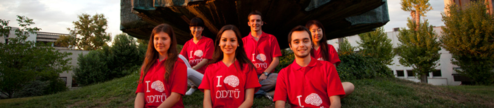
“Our facilities in METU are similar to the ones all across the world and we have equal opportunities and conduct the same level of research with most of the institutions in U.S., Europe and Asia”
“The article that was published in the newspapers was about growing zinc oxide nanowires in a commercial microwave oven that all of us are using in our kitchens….What we did is to heat up the solution in a microwave oven to decrease the time it takes to grow these nanowires. I came up with this idea while heating up my soup one day in a microwave oven at home. We found out that nanowires then grow in matter of minutes and they can be grown over large areas”
“And if one could grow nanowires within the matter of minutes over large areas for these applications that could be quite advantageous. Also imagine doing this with a simple and cheap microwave oven. We are also foreseeing and investigating other applications of zinc oxide nanowires in antireflective coatings, superhydrophobic coatings and sterilization. I believe that we can grow zinc oxide nanowires on any type of surface, and then we can find applications for them. The fact that particular applications will benefit from the properties of nanowires; is what we are trying to establish and demonstrate here in METU.”
Q: Thank you very much for accepting our interview request. Could we start with your academic career; how you have chosen this department and then specialized in the field of nanotechnology?
Dr. H. Emrah Ünalan: I would also like to thank you for inviting me to this interview. My choosing this department goes back to the nationwide university entrance examination, where I got accepted to the Department of Metallurgical and Materials Engineering at METU. The reason I like this major is that it is quite interdisciplinary and applicable to any type of engineering major, in addition to basic sciences like physics and chemistry. List of things you can work on with the broad background you get in this field include but are not limited to ceramics, polymers, metals, composites and advanced materials like biomaterials, electronic materials, nanomaterials.
I got into this department in 1997, it took me five years and I graduated in 2002. At the same year, I got accepted to the Department of Materials Science and Engineering at Rutgers University in the United States to pursue my PhD degree with a research assistantship. I worked on carbon nanotubes with my advisor Prof. Manish Chhowalla and I got my PhD degree in 2006. Immediately after, I started my post doctoral studies under the supervision of Prof. Gehan Amaratunga at the Department of Electrical Engineering at the University of Cambridge in England for. There, the first project I got involved with was supported by Samsung to develop nanoscale materials for electronics. In my second year, 2008, I started working in a joint project between Cambridge University and Nokia on developing flexible mobile phones. Our group was involved with the battery component and we were working on flexible batteries for mobile phones. Towards the end of 2008, I started my current position in the Metallurgical and Materials Engineering Department at METU.
And when it comes to specialization in nanotechnology; it is the revolution in materials science, this is how we call it. The properties of materials do change a lot when you decrease their size and this fascinates people, including myself. A lot of effort is devoted all over the world on producing nanomaterials, understanding their properties and exploring their applications. Nanomaterials were out there for dozens of years; however, it is only until recently tools have been developed to observe and characterize them. I was a bit involved with nanotechnology when I was an undergraduate here in this Department preparing my graduation project in my senior year. I was trying to make nanopowders to measure their hydrogen storage properties. Then, I literally became involved with nanotechnology during my PhD studies and afterwards. I worked on nanotubes and nanowires during my time in Rutgers and Cambridge, respectively. I would also like to add that my experience coincides with Turkey’s growing effort on nanotechnology and I am quite happy to take part in that.
Q: Since you have been abroad for while, how do you perceive Turkey’s position now in the field of nanotechnology? When you compare the situations in 2002 and 2008, or now, how do you evaluate the differences? Is there a remarkable progress in the quantity and quality of research conducted at universities, centers or industry?
This is actually a good question. I would like to give an example for that change in METU. In 2002, as I said, I was doing some research and therefore I was using the laboratories in our Department. Then, when I came back here in 2008, I got the opportunity to witness the change within those six years. The amount of research had increased exponentially. What I mean by research is facilities, number of thesis published, number of projects signed, number of papers published etc. This is probably related to the number of funds to available researchers and I believe back in the beginning of 2000s these funds were not as diverse in number and large in amount as they are today. And I believe this is not only happening in the field of nanotechnology.
I should also add that the Central Laboratory that we have here in METU, which was founded in late 2004, means a lot to us. It is very difficult to have the entire infrastructure required for your project available to you in your own laboratory. This is where the Central Laboratory comes in to the picture, because a lot of characterization facilities are available for us there. This not only minimizes the cost of analysis; but also saves time since we do not need to send samples elsewhere for measurement.
In such an environment, the first question I ask to students who would like to have an academic life and get a graduate degree abroad is: “Why do you want to go abroad?”. Our facilities in METU are similar to the ones all across the world and we have equal opportunities and conduct the same level of research with most of the institutions in U.S., Europe and Asia. So, the students have to first convince me on what the driving force is for them to go abroad. Otherwise, they could stay here at METU, get their Masters’ degree and could then decide upon getting their Ph.D. degree here or elsewhere.
Q: It seems important to highlight that students should be aware of their purpose in deciding to go abroad for graduate studies. As far as I understand, you are critical about going abroad just for doing so, especially while we have the same infrastructure and equipment in Turkey. So, are you suggesting that now in Turkey, more specifically in METU, students have more opportunities than you had at the beginning of the 2000s?
That’s exactly true and I do not see any point in going abroad for a Master’s degree. However, for a Ph.D.degree and especially if an academic life is sought, the situation could be different. This is mainly derived from the fact that some universities do mind inbreeding and require a Ph.D. degree or a post-doctoral experience pursued abroad. Hence, as said, one may prefer to go abroad for post-doctoral studies.
I would also like to add that when my Ph.D. advisor came to Turkey to give a talk in a conference, he had a chance to visit our department, the Central Laboratory and my laboratory. He was fascinated with our infrastructure, and told me that he was not expecting this much. In fact, this was back in 2009 and I am quite happy to say that we have further improved that infrastructure in the last 2 years.
Q: To turn back to your research, from the beginning of your Ph.D., which steps did you take? Which funds did you use in evolving your research?
I got funded for the first year of my Ph.D. with a research assistantship from Rutgers University. Then, from 2003 to 2006, I was funded by the startup grant of my Ph.D. advisor, because I was his first Ph.D. student. In Cambridge, my experience was a bit different. I got involved with a very big group and a well-set laboratory. As I said, the funds for the first year came from Samsung and in the second, Nokia provided support.
Q: I would like to continue with the national funds that you got when you came back to Turkey, but let me first ask whether you have continued to work on the same specific field or you have altered your focus over time…
During my time in Rutgers, I worked on carbon nanotube thin films. I started with the synthesis of carbon nanotubes and proceeded with their purification, dispersion, deposition onto a substrate in the form of a thin film, characterization of the thin film properties and fabrication of devices using those thin films. By the time we started making carbon nanotube thin films, just a few research groups in the U.S. were working on this. However, after only 5-6 years, there are now companies producing carbon nanotube thin films at industrial scale and many other research groups involved in this research.
At this point let me introduce you to carbon nanotubes. The black part of a pencil is graphite, which is constituted of individual layers, called graphene, stacked on top of each other in atomic scale. If we take one of these graphene layers and roll it up to form a cylinder we end up with a carbon nanotube. The one with only one cylinder is our interest, which is called single-walled carbon nanotube. Single-walled carbon nanotubes have a diameter of around one nanometer, equal to the billionth of a meter, and their length ranges from several hundreds of nanometers to a few microns.
Fantastic electrical, optical and mechanical properties were reported using individual carbon nanotubes. I am interested in electronic devices and in order to fabricate devices with only one single carbon nanotube you need to use intense, delicate and time-consuming processing steps. This makes it impractical and limits commercial applications. Our intention at that stage was to make carbon nanotube thin films, in which you use thousands and thousands of nanotubes in an ensemble behavior, similar to a spider web. You end up sacrificing a bit in performance; but gain a lot in processability. This also means that one can make large area devices. Since the thin film fabrication process takes place almost at room temperature, one can use flexible substrates for their deposition, which would at the end allow the fabrication of flexible devices. In fact, they are also transparent. We have used carbon nanotube thin films in transistors and transparent conducting electrodes for solar cells.
In Cambridge, I started working with nanowires. Nanowires have similar lengths with carbon nanotubes, yet are a bit larger in diameter. They can also be in various chemistries ranging from elemental ones to oxides and nitrides. I started working on zinc oxide nanowires. Originating from the Rutgers experience, my intention in Cambridge was to use the thin film concept. So again, instead of using only one zinc oxide nanowire, we used a lot of them together and made zinc oxide nanowire thin film devices in the scope of the Samsung project. Zinc oxide is transparent and in the nanowire form it allows the fabrication of both transparent and flexible devices. We may realize the transparent screens in the famous movie Avatar at some point in the future; maybe even the flexible ones. Then, I went back to working on carbon nanotubes in my second year, where we developed carbon nanotube-based flexible batteries for Nokia. In fact, that project is still going on.
If we get back to your question, whether I am doing exactly the same thing here in METU: I am closely following what I did for my post-doctoral work in Cambridge. Right after setting up the laboratory, we first started with the growth of zinc oxide nanowires, here in METU. Other chemistries of nanowires interest to us are silver, silicon and germanium.
Two of my projects are funded by TÜBİTAK; one of them is on the fabrication of light emitting diodes (LEDs) with zinc oxide nanowires and the second one is on nanowire-enhanced solar cells. One needs to produce nanomaterials in large quantities if an application is sought. Therefore, my intention here at METU is to synthesize nanowires and nanotubes in large quantities; because, if you are going to use them in any sort of application you need a lot of them. For the production of nanomaterials, we follow two approaches. The first one is the bottom-up approach, where you start with the building blocks, basically atoms, and assemble them together to produce your nanomaterial of interest. In the second approach, called top-down, bulk materials are refined down to nanomaterials using physical or chemical procedures.
One good thing with zinc oxide nanowires is that you can grow them at low temperatures in water. This makes the process really economic and scalable. If one thinks of LEDs and solar cells in the market, they are fabricated in vacuum using intricate equipments. What we intend to do in our laboratory is to use simple equipment, low temperatures and fabricate those devices even over a benchtop.
Q: There was news about your research which was about microwaves…
The article that was published in the newspapers was about growing zinc oxide nanowires in a commercial microwave oven that all of us are using in our kitchens. Zinc oxide nanowire growth takes place in a water solution with necessary chemicals. That solution needs to be heated up to around 90°. The only disadvantage of this growth is that it takes place in hours or days. What we did is to heat up the solution in a microwave oven to decrease the time it takes to grow these nanowires. I came up with this idea while heating up my soup one day in a microwave oven at home. We found out that nanowires then grow in matter of minutes and they can be grown over large areas. We have also demonstrated that nanowires can be patterned beforehand, if further intention is to use them in devices.
Q: Will this discovery have a direct impact on people’s life, I mean will the cheap and quick growing of nanowires have implications in our daily lives?
We already use zinc oxide in powder form in very many places. List of applications include but are not limited to paint, cosmetics, sunscreens and lubrication. Since it is used widely, we don’t have problems with the accessibility of the precursor chemicals for the production of nanowires. Nanowires provide advantages like single crystallinity and contain fewer or almost no defects compared to powders or thin films. This becomes important if you are making an optoelectronic device such as a solar cell or a LED. Fewer defects within the nanowires means one could fabricate LEDs that are brighter or solar cells with higher efficiencies.
And if one could grow nanowires within the matter of minutes over large areas for these applications that could be quite advantageous. Also imagine doing this with a simple and cheap microwave oven. We are also foreseeing and investigating other applications of zinc oxide nanowires in antireflective coatings, superhydrophobic coatings and sterilization. I believe that we can grow zinc oxide nanowires on any type of surface, and then we can find applications for them. The fact that particular applications will benefit from the properties of nanowires; is what we are trying to establish and demonstrate here in METU.
Q: To continue from here, what are your plans in METU? You have just initiated a laboratory, what will be the following steps?
In August, it will be three years since I have moved back to METU. In these three years with the funds that I got; the two TÜBİTAK projects that I have already talked about and another one that I have involved with which is sponsored by State Planning Organization (SPO) “Center for the Solar Energy Research and Application Fund” and a couple of Scientific Research Projects (BAP) funded by METU, I and my students have tried to set up our laboratory. This includes setting up the work space, purchasing and setting up equipments etc. We are still waiting for a few more equipment that will be installed in our laboratory. Let me also remind you that we are doing experimental research. This necessitates equipment, students and consumables at a wide extent. As a following step, I will look for some industrial partners to work with, similar to my Samsung and Nokia experience in Cambridge and definitely start applying for international projects.
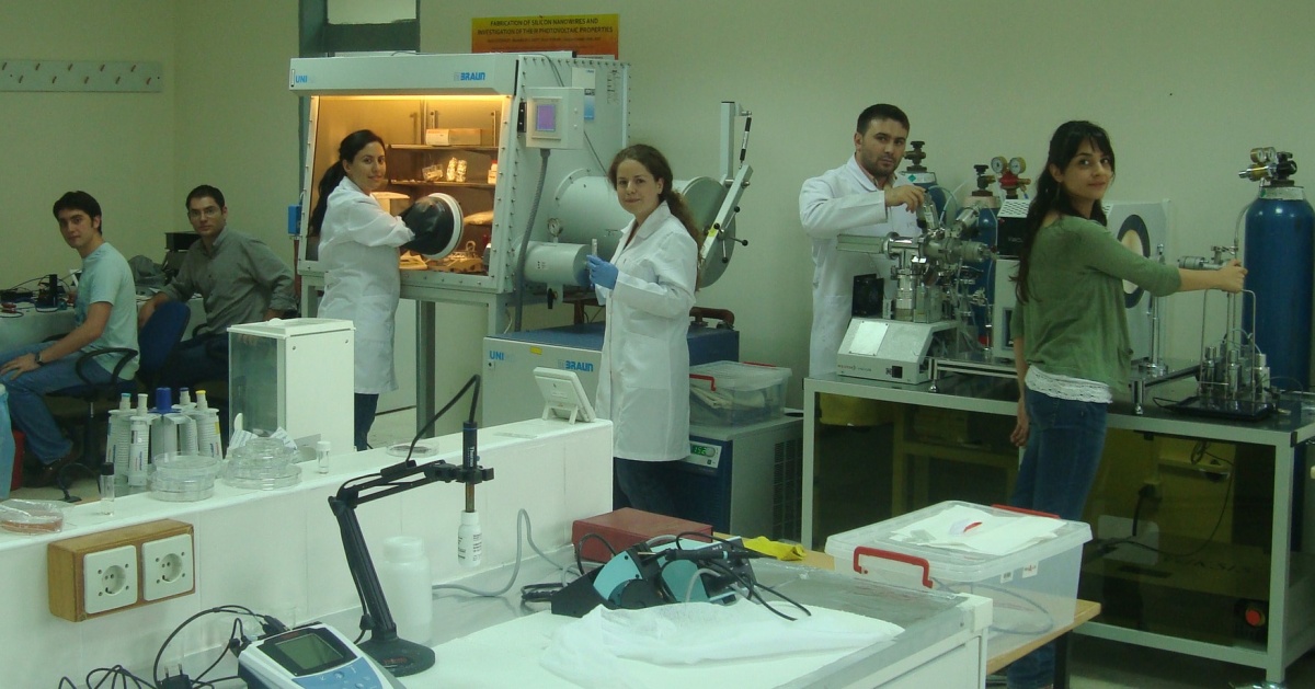
Q: You have said that students are very important for conducting research. Are your students interested in these projects and working in the lab? Please tell us about your research team in METU. When you compare it to the environment that you have experienced abroad, how is the interest of students here?
In the U.S., it was a different experience because I was the first Ph.D. student of my advisor. We set up everything from scratch. It helped me in the sense that I did exactly the same thing here in METU and made use of my experience I had there.
In terms of students, I am quite happy to say that there are so many students who apply to me for getting a Master’s or Ph.D. degree. And I believe this is because they are interested in what I am doing. For undergraduates, our department is offering a two semester, total of 3 credit course, called Undergraduate Research I and II. This is for them to get involved in laboratory work and get some hands-on experience. With this intention, every year I get two to three undergraduate students working in my lab. They can work on a small portion of one of the funded projects I am conducting or they can work on something totally different in which the student is interested in. For example, with one of the students we tried to extend the life of flowers using silver nanoparticles. With another student of mine, we tried to make superhydrophobic textile surfaces using zinc oxide nanowires.
Students are intelligent and enthusiastic about learning, which is very motivating for me.
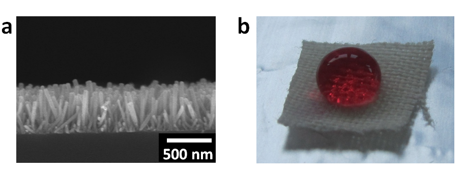
The figure above presents electron microscopy image of zinc oxide nanowires in (a) and superhydrophobic nature of zinc oxide nanowires on textile surfaces on (b), similar to a lotus leaf.
Q: How many graduate students do you have now?
In addition to Metallurgical and Materials Engineering, I am also involved in the Micro and Nanotechnology Program at METU. This allows me to attract students from both programs. I have six Master’s and two Ph.D. students actively working in my laboratory. They have different backgrounds and, as I said before, nanotechnology is quite interdisciplinary. Some of the students are coming with physics background, some of them with chemistry background and I also would love to have students with electrical engineering or biology background. I believe this is the only way to get fruitful results at the end.
Q: So, at the level of students you are encouraging interdisciplinary studies. Do you also have collaborations with other departments in your projects?
Definitely! The materials science program itself is interdisciplinary. But if a student wants to go beyond that, there are double major and minor undergraduate programs available. In fact, quite a few of the undergraduate students in our department are already involved with those programs.
When it comes to graduate students, the Micro and Nanotechnology Program works in that respect. This program necessitates that the advisor and the co-advisor of the students must be from different disciplines. In that sense, we are cooperating with the Physics and Chemistry Departments. The Physics Department is also leading the GÜNAM Project, which I am also involved in. We are trying to develop solar cells with silicon nanowires within the scope of this project.
For the synthesis of silicon nanowires, in literature, quite a lot of people used high temperature bottom-up approaches that necessitate vacuum systems. Vacuum and high temperatures are quite costly processes. For a solar cell application, we are talking about areas of m2 to km2 of active material. Therefore, the growth method utilized needs to be cheap, easy and widely available. With that objective, we are fabricating silicon nanowires via a top-down approach using simple electroless etching method. By this method, we are not experiencing problems with the electrical properties of the nanowires, since we know the properties of our starting wafer. This is quite a big problem in bottom-up approaches. Our process takes place at temperatures lower than 50°C and is not size limited. Thus, with one shot we fabricate nanowires with the desired properties over large areas which are then used in solar cells.
Q: We have so far talked about national projects. Do you want to take part in international projects?
Unfortunately, I missed the opportunity for the Marie Curie Reintegration Grant. This is because I had already been to Europe during my time at Cambridge.
National funds are more achievable for new researchers; international projects might then follow. Over the last 3 years, my intention was to establish the laboratory here in METU. Only after this, the following step would definitely be the application to an EU project. I believe my Cambridge experience would help me a lot on finding project partners in Europe.
Q: Lastly, let me ask about being a young researcher in METU; how would you evaluate the opportunities and the defects of METU in the field of research especially for a young researcher? You have graduated from METU, but after spending time abroad as a researcher, why did you prefer to come back to Turkey, to METU and especially to this department?
I do enjoy being a researcher here and I think I am already over the hardest part of initiating a research group. METU means a lot to me, it is like my home, where I got my Bachelor’s degree. This is the main reason why I came back to initiate my laboratory and a research team. Working in close contact with your own professors is also quite an encouraging and a stimulating experience. METU is the right place in terms of the infrastructure it provides, its reputation and vision. I feel that I am at the right place to realize my goals. And I hope to contribute positively to this environment.
We also have no problems of finding students to work with. METU is again the right place, since it is good at publicizing research opportunities, as well providing support during the application process. For example, I got the TÜBA-GEBİP award in 2009. I heard about this award and a few other projects that I could apply to during the Research Info Series regularly organized by METU.
Publication and performance awards and travel supports are a few other advantages that I could add. There is also an internal small start-up grant for new researchers. This has nothing compared to start-ups in the U.S. and Asia; but provides you some support at the beginning of your academic life. It provides a good starting point to initiate research. Actually, the only deficiency I can think of is the absence of decent sized start-up grants. This is valid not only for METU; but probably also for all the other universities in Turkey. Big start-up grants would be beneficial in the early stages of academic life.
Q: Thank you very much for accepting this interview….